
Low-Temperature Conductivity in Cu-doped CeO2 Nanoparticles
Date:
Low Temperature Electronic Properties of nano Cu-doped CeO2.
See the poster here!
Since the summer of 2022, I have worked in the lab of Dr. Siu-Wai Chan on the synthesis and EIS (electrochemical impedance spectroscopy) characterization of nanoparticles of copper-doped cerium oxide. My goal for this page is to serve as a reference for the analysis of my results and the production of figures and tables for my senior design expo (SDE) poster. Not all aspects of the project and my work are contained here, however. For details regarding sample synthesis and preparation, I have maintained a lab notebook during my time in the Chan lab.
Many thanks are due to my wonderful lab partner and graduated Columbia SEAS EE master’s student, Yanhe Li.
Synthesis and Sample Preparation
The synthesis of ceria nanoparticles involves a 1310 minute co-precipitation reaction as outlined below:
Reactants:
- Cerium(III) nitrate hexahydrate, Ce(NO3)3•6H2O: $6.5133g$
- HMT, hexamethylenetetramine, (CH2)6N4: $28.0372g$
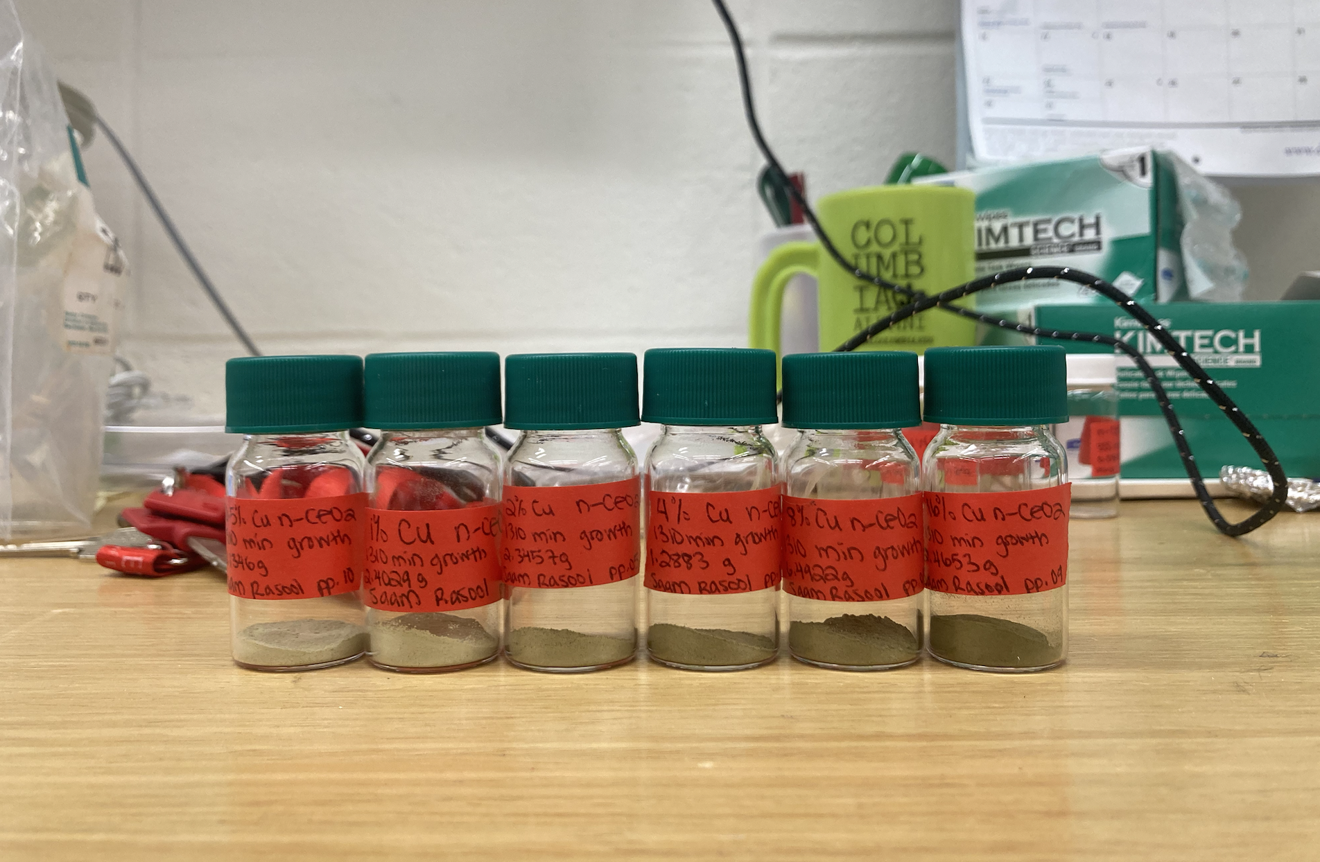
- Copper nitrate hexahydrate, Cu(NO3)2•2.5H2O: $n•0.046525g$, when trying to produce $n\%$ Cu-CeO2.
- Deionized water (18 MΩ)
(This will yield approximately $2.4g$ of nanoparticulate powder)
Synthesis:
- Ensure that the lab temperature is 26°C
- Dissolve both the cerium nitrate and HMT in deionized water (in separate beakers) to create a $400mL$ solution
- Add the copper nitrate to the cerium nitrate solution
- Stir both beakers for 30 minutes
- Combine the contents of each beaker and stir for 20 minutes
- Move the mixture to a 40°C water bath and stir for 3 hours. Cover the top of the beaker with tin foil
- Remove the mixture from the water bath and stir for 18 hours
- Dry the beaker, cover with aluminum foil, and refrigerate to stop the growth of particles
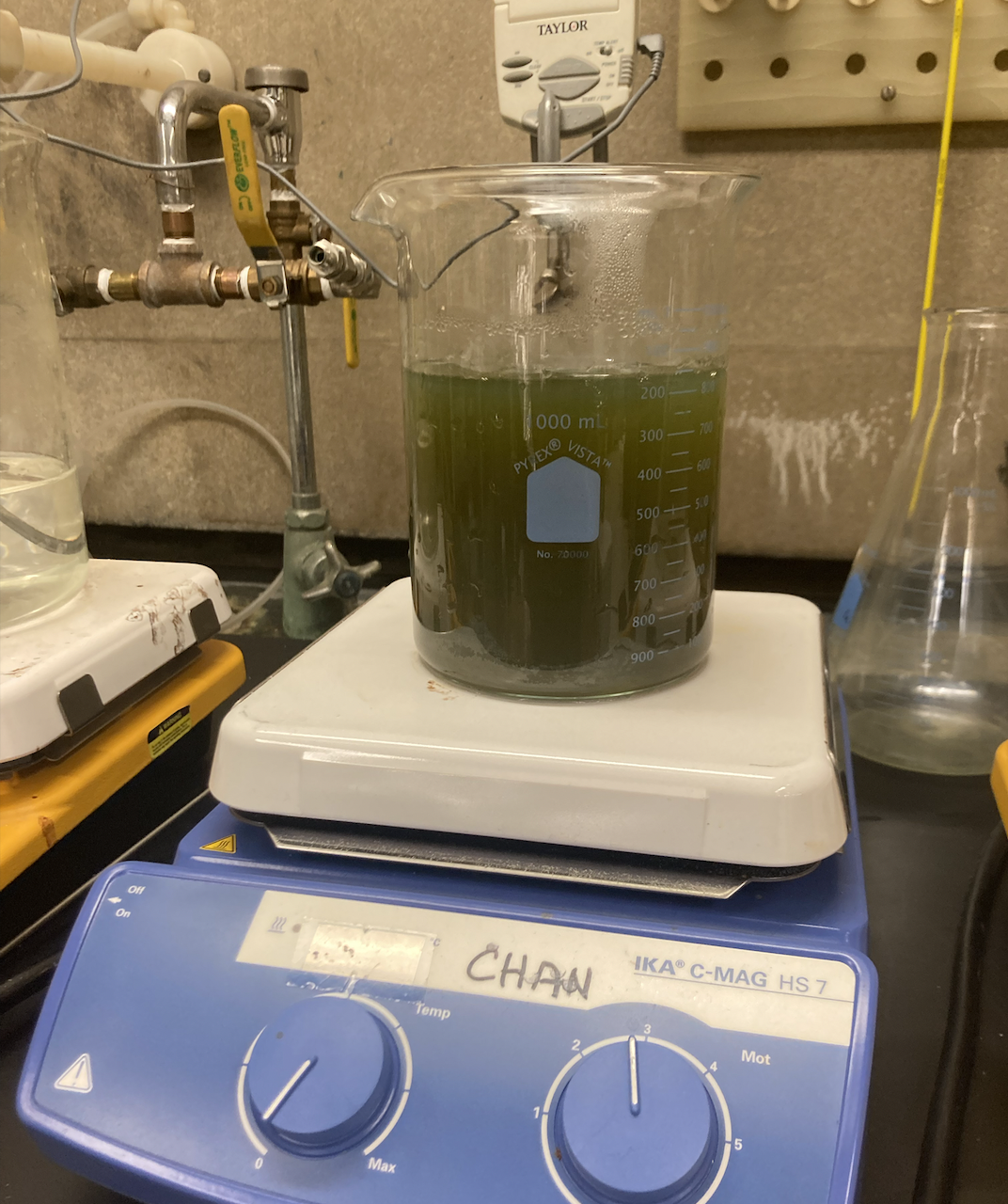
- Pour the nanoparticles into two centrifugation bottles and label. The excess solution may be discarded in chemical waste containers. Do not fill the centrifugation bottles more than one-third full
- Centrifuge the nanoparticles at 5°C for 2 hours at 12500 rpm
- Discard excess water from the centrifugation bottles
- Place the uncovered bottles in a bin and cover the bin with tin foil. Let the nanoparticles dry for at least three days
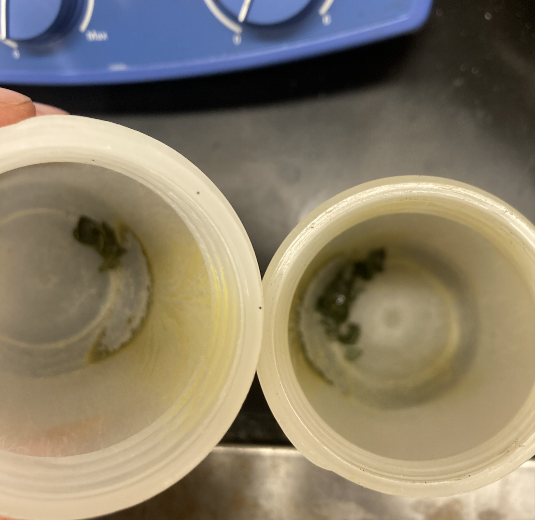
- Scrape the nanoparticle shards from the centrifugation bottle and crush into a fine powder with a pestle and mortar for 10 minutes
- Weigh and label a glass vial containing the nanoparticulate powder
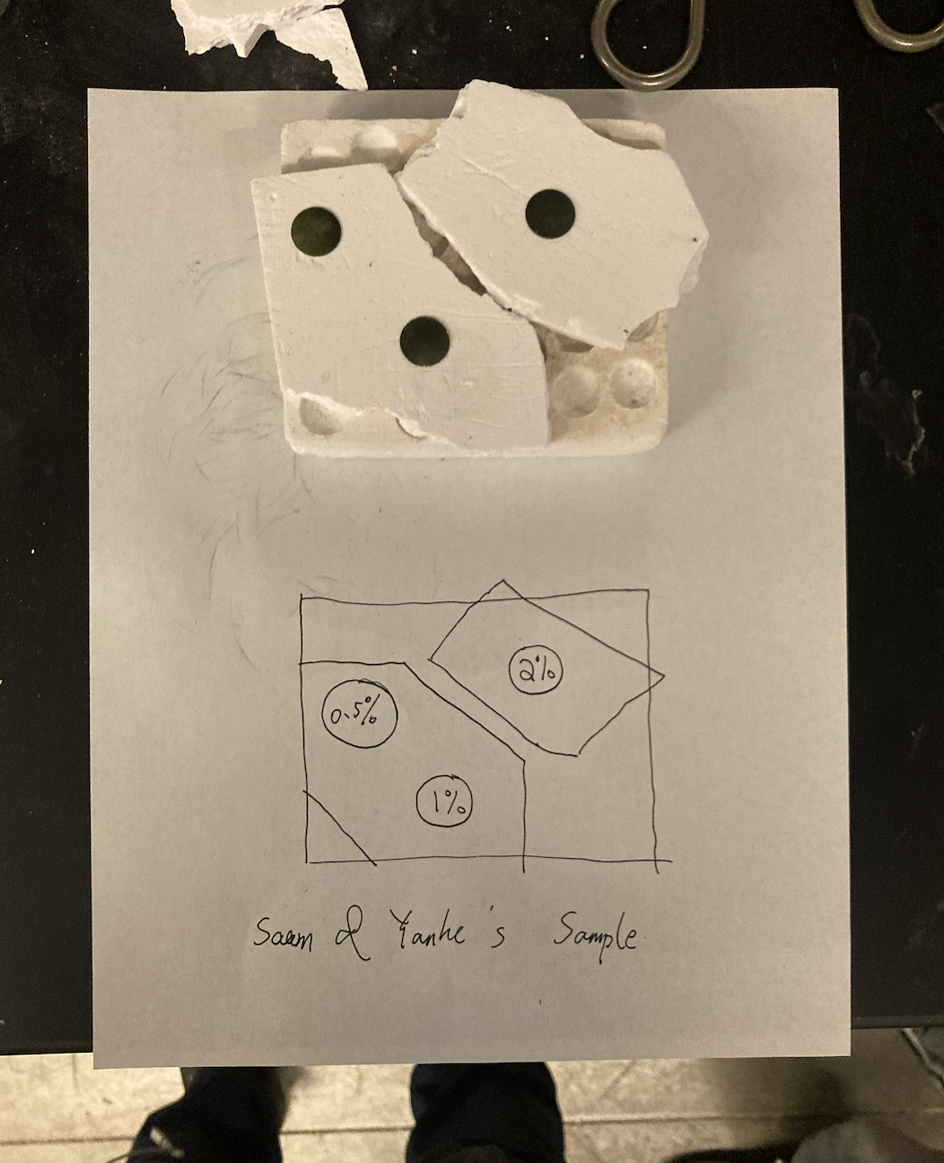
Pellet pressing:
Much of the pellet preparation work was done at Columbia’s Lamont-Doherty Earth Observatory in NJ in the geoscience lab of professors Yves Moussallam and David Walker, and under the supervision of their lab manager Shuo “Echo” Ding. Many thanks are owed to each of them for their generosity and supervision in our sample preparation process. I also need to thank Yanhe for driving us and our nanoparticles across the George Washington bridge all those times.
The die for uniaxial pressing of our pellets may need to be explained in more detail here before listing the procedural steps below. The die consisted of the upper and lower housing (the lower is black and the upper is silver), two small central cylinders, and one longer central cylinder meant to contact the hydraulic press arm. The two small inner cylinders are to be in contact with the powder, and intentionally dented such that one can ensure that indented sides are in contact with the powder while the smooth sides face away from it.
- Assemble the die chamber, placing the silver housing firmly on the black housing until a connection is made
- Insert the first small cylinder into the chamber dented side up
- Deposit $0.170g$ of powder into the chamber. Try to distribute the powder to obtain a layer of uniform thickness
- Insert the second small cylinder into the chamber dented side down
- Insert the longer cylinder into the chamber with the beveled edge sticking out
- Run a finger along the edge where the two housings meet. If you can fit a fingernail between them, there is air trapped in the die and the two housings need to be pushed together completely to ensure that full pressure will be applied to the powder
- Tap the die on a flat surface to ensure (again) that the powder has uniform thickness
- Bring the die to the ENERAC, an oil-based hydraulic pump and press. Place the die in the center of the hydraulic press arm
- Turn the oil valve to the closed position. Ensure it is all the way closed
- Lower the hydraulic arm until it is touching the sample and incrementally increase the pressure to 5000 psi
- Wait approximately 10 minutes until the pressure has decreased to about 2000 psi. Then, very slowly release the pressure until the hydraulic arm begins to lift from the die
- Turn the die upside down and place a small acrylic shield around the top in order to push out the central cylinders. Lower the hydraulic arm very carefully until the top housing barely makes contact with the press stage
- Remove the small cylinder that is now fully exposed and carefully remove the pellet with a razor blade
- Disassemble and thoroughly clean all parts of the die with a Kimwipe or paper towel and isopropyl alcohol
- If the pellet is broken, label and keep it for re-powderization
Pellet heat treatment:
The pellets are now heat treated to evaporate any HMT still present in the pellet. The furnace used was controlled by a Eurotherm temperature controller and the heating program performed is as follows:
- ramp 1: 120°C/h
- level 1: 350°C
- duration 1: 4h
- ramp 2: 120°C/h
- level 2: 0°C (This will only cool the pellet to room temperature)
- duration 2: $\infty$
To run the program, press the middle button. To kill the program hold both side buttons. The pellets should not rest directly on the furnace floor, but on a piece of thermally insulating material.
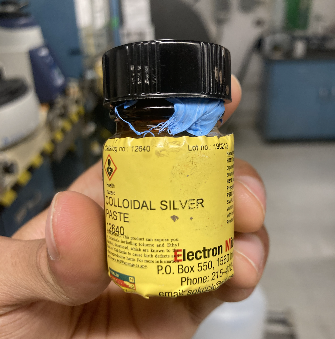
Electrode painting:
The following procedure was carried out with the help of Adrian M. Chitu in the MSE teaching lab. He also provided me with the colloidal silver paste used to produce the conductive electrode surface.
- Using a paintbrush or a q-tip, apply colloidal silver paste thinly onto the top surface of each pellet being careful not to paint onto the sides
- Let dry for 2 hours
- Prepare a microscope slide with a conductive track of electrode paste, about 2cm long
- Apply a dab of Ag paste to one end of the track. Flip the pellet and place such that the painted side touches the dab but some of the conductive track is still exposed
- Let dry for 2 hours
- Cut gold wire into 5cm long sections. 2 are needed for each pellet. Dip one end of each wire into the Ag paste to improve the cohesion between wire and pellet/track
- Paint the other side of the pellet, being careful not to create a short-circuit
- Dry for 2 hours
- Using a few dabs of conductive paste, attach the painted ends of the wires to the top face of the pellet and the end of the conductive track. Fully cover the wires in paste and let dry

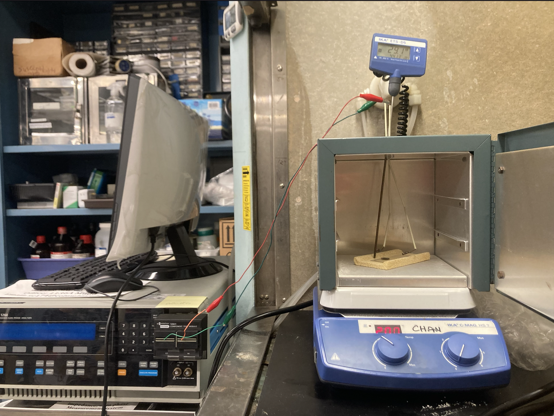
Test setup:
- Place the pellet and its glass slide into the box furnace atop a piece of porous ceramic material
- The box furnace should have a hole in its top through which a thermometer and two copper wires protected by an alumina sleeve are inserted
- Snake the ends of each gold wire through the holes in the connections at the end of each copper wire
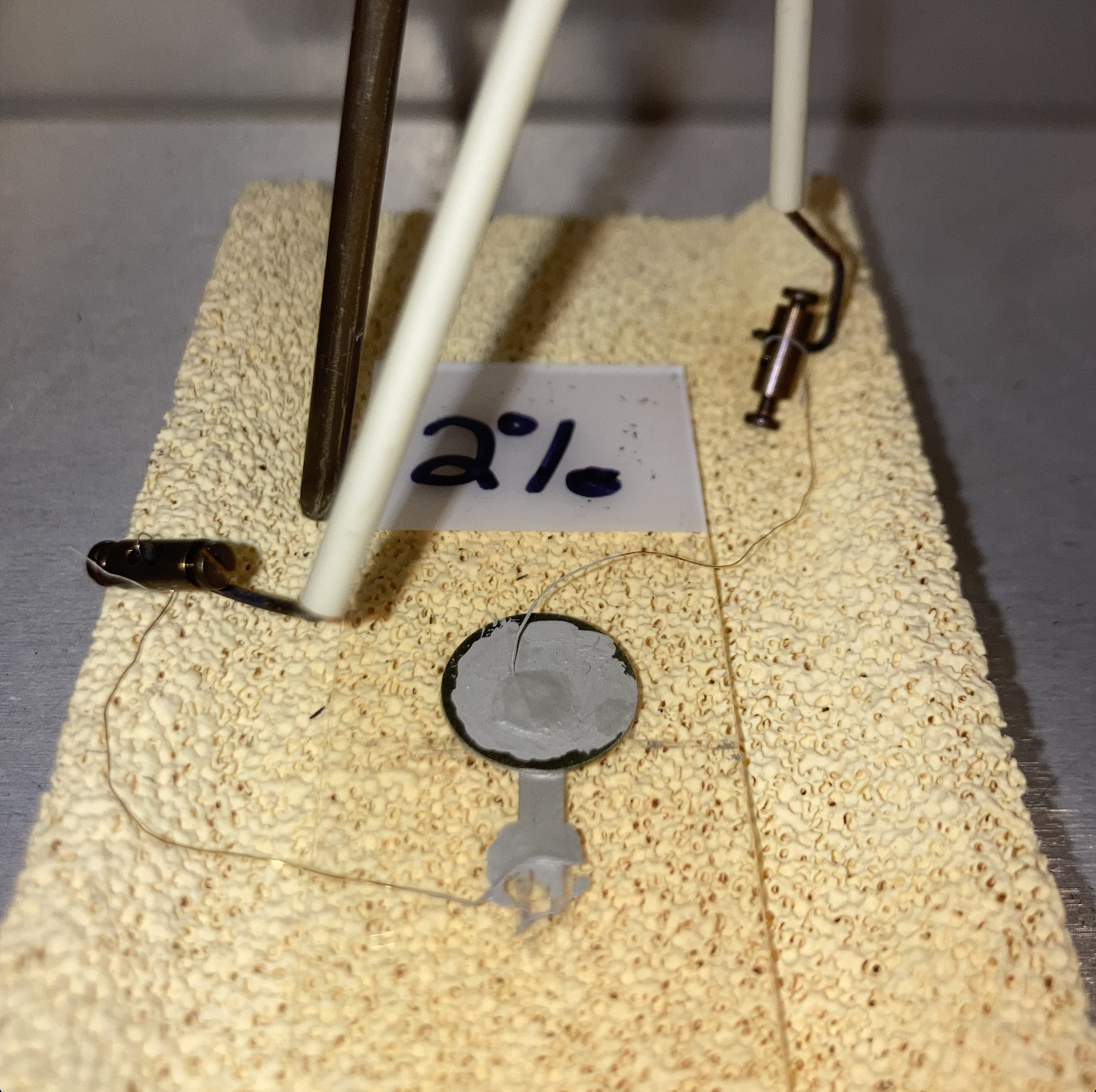
- Outside the furnace, connect the two wires to the input ports of the Solartron impedance analyzer
Analysis
EIS Data Plotting How-To:
I created the below code to present the EIS data using matplotlib to give myself greater control over the presentation and formatting.
The code reads from a folder containing .txt files outputted from the EIS visualization and equivalent circuit fitting software ZView (version 3.2).
To obtain these preformatted .txt files, I saved EIS data from the Solartron (an impedance analyzer) to .csv files. Within the .csv file, I converted the impedance magnitude and phase angle (polar) to real and imaginary impedance. From this point, I organized the data such that the columns for AC frequency, Re(Z), and Im(Z) were adjacent (and in that order).
I then create a .txt file with the same name as the Solartron EIS data and copy those three columns into it. The result should be delineated by spaces (i.e. does not require further formatting) and contain as many new lines as data points. We can then load this .txt within ZView where it will produce Nyquist and Bode plots for our data. Rescaling the charts is neccesary to see the data fully.
Within ZView it is possible to remove outlying or nonsensical data, which was useful in separating the high frequency data from the low frequency data. At this point, saving the workspace file will produce a preformatted .txt file that appears in the same directory as the simple 3-column .txt file.
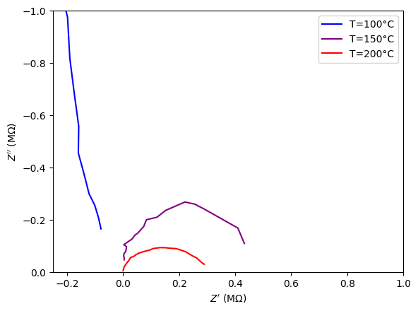
To use this code, put these preformatted .txt files into a folder and reference them with the os.chdir() function. In this implementation, I label them such that from top to bottom, they correspond to test temperatures of 100°C, 150°C, and 200°C.
# importing matplotlib module
import matplotlib as mpl
import numpy as np
from matplotlib import pyplot as plt

import os
os.chdir("/Users/saam/Documents/n-Cu-CeO2 Research/Python Files/8%ZViewTxtsEdited")

# obtains Z' and Z'' line-wise
def lines(lineno):
    file.seek(0)
    return file.readlines()[lineno]

def getNyquist(line):
    data = list(lines(line).split(", "))
    # converts to M*Ohm
    data = [float(i)/1000000 for i in data]
    return data[4:6]

# introduce the axis first
fig, zzplot = plt.subplots()

# changes the default color cycle and resolution
mpl.rcParams['axes.prop_cycle'] = mpl.cycler(color=["blue", "purple", "red"])
mpl.rcParams['figure.dpi'] = 100
mpl.rcParams['font.family'] = 'DejaVu Sans'

# temperature parameter, please excuse my coding ineptitude
T = 100

for filename in sorted(os.listdir(os.getcwd())):
    Z_R = np.array([])
    Z_IM = np.array([])

    with open(os.path.join(os.getcwd(), filename), 'r') as file:
        for lineno in range(11,len(file.readlines())):
            Z_R = np.append(Z_R, getNyquist(lineno)[0])
            Z_IM = np.append(Z_IM, getNyquist(lineno)[1])
    zzplot.plot(Z_R, Z_IM, label = 'T='+str(T)+'°C')
    T += 50

zzplot.invert_yaxis()
zzplot.ticklabel_format(useOffset=False, style='sci')
plt.xlabel('$Z\'$ (MΩ)')
plt.ylabel('$Z\'\'$ (MΩ)')
plt.gca().set_xlim(-0.25,1)
plt.gca().set_ylim(0,-1)
plt.legend();
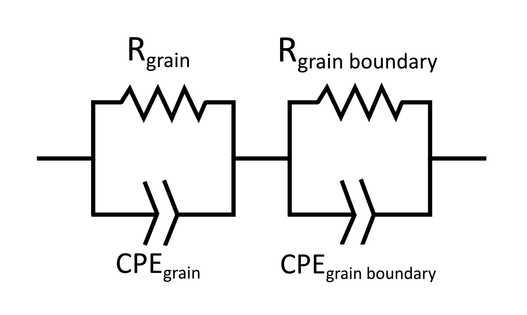
The Equivalent Circuit
ZView was neccesary for this project as a fitting tool for EIS curves generated by an equivalent circuit diagram. This functionality can be accessed using the “Equivalent Circuit” tool in the main toolbar of ZView.
For the AC response of our samples, the generally agreed upon configuration is two parallel resistor/constant phase element (CPE) blocks in series. One representing the grain resistance and capacitance, and the other reprsenting the grain boundary resistance and capacitance. This is shown in the figure below.
from IPython.display import Image
Image("/Users/saam/Documents/n-Cu-CeO2 Research/Images and Figures for Poster/equivcirc3edit.jpeg", width = 600)
The CPE is a two-parameter component used in equivalent circuit modeling to describe an imperfect capacitor, or nearly capacitor-like behavior. It is often used to model the AC response of an electrical double layer. The impedance of a constant phase element is given by:
\[Z_{CPE}=\frac{1}{Q_0(i\omega)^n} \tag{1}\]- $Z_{CPE}$: complex impedance of a constant phase element
- $Q_0$: parameter with units $S•s^n$ (Siemens-seconds to the nth power)
- $i$: the imaginary unit
- $n$: a number between 0 and 1, (although ZView sometimes assigns a value slightly greater than 1)
- $\omega$: angular frequency of the AC signal, = $2\pi f$
When $n$ = 1, the CPE becomes a pure capacitor, and when $n$ = 0, it is equivalent to a pure resistor (in terms of impedance). For our data, we expect n values close to 1. Using this information we can deduce the impedance of a resistor:
\[Z_{R}=\frac{1}{Q_0(i\omega)^0}=R \tag{2}\]When $n$ = 0, $Q_0$ becomes the electric admittance, with units Siemens. Therefore, the impedance of a resistor is simply the resistance.
In a circuit, impedance is calculated in the same way as resistance, i.e. added in series and taking the reciprocal of the sum of reciprocal terms when in parallel. Therefore, for the above circuit, (letting g represent grains, and gb represent grain boundaries) we will have an impedance given by:
\[\frac{1}{Z_{g}}=\frac{1}{R_{g}}+Q_{0_{g}}(i\omega)^{n_{g}} \tag{3}\]and
\[\frac{1}{Z_{gb}}=\frac{1}{R_{gb}}+Q_{0_{gb}}(i\omega)^{n_{gb}} \tag{4}\]and therefore:
\[Z=\frac{1}{\frac{1}{R_{g}}+Q_{0_{g}}(i\omega)^{n_{g}}} + \frac{1}{\frac{1}{R_{gb}}+Q_{0_{gb}}(i\omega)^{n_{gb}}} \tag{5}\]| See that $(i\omega)^{n}=\omega^ni^n=\omega^n e^{ln(i^n)}=\omega^n e^{n(ln(i))}$, and $ln(i)=ln | i | +i(Arg(i))=\frac{i\pi}{2}$, so $(i\omega)^{n}=\omega^n e^{\frac{ni\pi}{2}} =\omega^n (\cos(\frac{n\pi}{2})+i\sin(\frac{n\pi}{2}))$. |
Solving each fraction separately first, then combining gives us the following analytic parameterization for Z:
\[\Re(Z)=Z'=\frac{\frac{1}{R_{g}}+Q_{0_{g}}\omega^{n_{g}}\cos(\frac{n_{g}\pi}{2})}{\frac{1}{R^2_{g}}+\frac{2Q_{0_{g}}\omega^{n_{g}}}{R_{g}}\cos(\frac{n_{g}\pi}{2})+Q^2_{0_{g}}\omega^{2n_{g}}} + \frac{\frac{1}{R_{gb}}+Q_{0_{gb}}\omega^{n_{gb}}\cos(\frac{n_{gb}\pi}{2})}{\frac{1}{R^2_{gb}}+\frac{2Q_{0_{gb}}\omega^{n_{gb}}}{R_{gb}}\cos(\frac{n_{gb}\pi}{2})+Q^2_{0_{gb}}\omega^{2n_{gb}}} \tag{6}\] \[\Im(Z)=Z''=-\frac{Q_{0_{g}}\omega^{n_{g}}\sin(\frac{n_{g}\pi}{2})}{\frac{1}{R^2_{g}}+\frac{2Q_{0_{g}}\omega^{n_{g}}}{R_{g}}\cos(\frac{n_{g}\pi}{2})+Q^2_{0_{g}}\omega^{2n_{g}}} - \frac{Q_{0_{gb}}\omega^{n_{gb}}\sin(\frac{n_{gb}\pi}{2})}{\frac{1}{R^2_{gb}}+\frac{2Q_{0_{gb}}\omega^{n_{gb}}}{R_{gb}}\cos(\frac{n_{gb}\pi}{2})+Q^2_{0_{gb}}\omega^{2n_{gb}}} \tag{7}\]In particular, this parameterization will give us the sum of two circles, each shifted by a constant along the real axis.
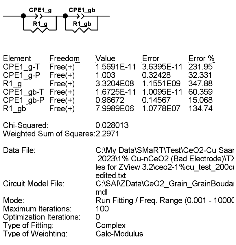
The following image provides an example of the fitted parameters ZView provides, along with the associated goodness of fit for each parameter. Note that in the image, the “T” component of the CPE corresponds to $Q_0$, and the “P” component corresponds to $n$.
from IPython.display import Image
Image("/Users/saam/Documents/n-Cu-CeO2 Research/Images and Figures for Poster/zviewfit.png", width = 600)
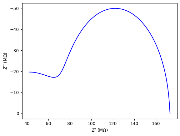
The below code makes a plot of the fitted parameterized EIS curve given the six relevant parameters. I am using equation (5) to generate the data points since python has support for math with complex numbers. It may be useful to overlay the fit on the raw data given by the first figure.
import cmath

#impedance of the grain/grain boundary modeled system, equation (5)
def z(w, r_g, q_g, n_g, r_gb, q_gb, n_gb):
    wi = w*(0 + 1j)
    return 1/((1/r_g)+(q_g*(wi)**n_g)) + 1/((1/r_gb)+(q_gb*(wi)**n_gb))

def re_z(w, r_g, q_g, n_g, r_gb, q_gb, n_gb):
    return np.real(z(w, r_g, q_g, n_g, r_gb, q_gb, n_gb))

def im_z(w, r_g, q_g, n_g, r_gb, q_gb, n_gb):
    return np.imag(z(w, r_g, q_g, n_g, r_gb, q_gb, n_gb))

#real impedance of the grain/grain boundary modeled system, equation (6)
#def re_z(w, r_g, q_g, n_g, r_gb, q_gb, n_gb):
#    return ((1/r_g)+(q_g*w**n_g)*np.cos(n_g**np.pi/2))/((1/r_g**2)+(2*q_g*w**n_g/r_g)*np.cos(n_g*np.pi/2)+q_g**2*w**(2*n_g)) + ((1/r_gb)+(q_gb*w**n_gb)*np.cos(n_gb**np.pi/2))/((1/r_gb**2)+(2*q_gb*w**n_gb/r_gb)*np.cos(n_gb*np.pi/2)+q_gb**2*w**(2*n_gb))

#imaginary impedance of the grain/grain boundary modeled system, equation (7)
#def im_z(w, r_g, q_g, n_g, r_gb, q_gb, n_gb):
#   return -((q_g*w**n_g)*np.sin(n_g**np.pi/2))/((1/r_g**2)+(2*q_g*w**n_g/r_g)*np.cos(n_g*np.pi/2)+q_g**2*w**(2*n_g)) - ((q_gb*w**n_gb)*np.sin(n_gb**np.pi/2))/((1/r_gb**2)+(2*q_gb*w**n_gb/r_gb)*np.cos(n_gb*np.pi/2)+q_gb**2*w**(2*n_gb))

#ac frequency
w = np.logspace(-5, 5, num=500, base=10)

#nyquist plot
plt.plot(re_z(w, 9.32*10**7, 1.569*10**-11, 1.003, 8*10**7, 1.673*10**-11, 0.567)/1000000, im_z(w, 9.32*10**7, 1.569*10**-11, 1.003, 8*10**7, 1.673*10**-11, 0.567)/1000000)

#let's scale and display them similarly to our first plot (M*Ohm)
plt.gca().invert_yaxis()
#plt.gca().set_xlim(0,9)
#plt.gca().set_ylim(0,-14)

plt.xlabel('$Z\'$ (MΩ)')
plt.ylabel('$Z\'\'$ (MΩ)')
Important note:
In the below tables, when the grain and grain boundary resistances were close in value (less than an order of magnitude), an equivalent circuit model with only one resistor and CPE was used. This was done to avoid reporting artificially low lattice reistances.
| T (°C) | $R_{g}$ $(MΩ)$ | $Q_{0_{g}}$ $(S•s^n)$ | $n_{g}$ | $R_{gb}$ $(MΩ)$ | $Q_{0_{gb}}$ $(S•s^n)$ | $n_{gb}$ |
|---|---|---|---|---|---|---|
| 100°C | $3.0712$ | $2.2279•10^{-11}$ | $1.121$ | $0.26337$ | $1.7067•10^{-10}$ | $0.92284$ |
| 150°C | $1.9824$ | $2.469•10^{-12}$ | $1.062$ | N/A | N/A | N/A |
| 200°C | $1.7551$ | $3.540•10^{-12}$ | $1.033$ | N/A | N/A | N/A |
Nanoparticulate 2% Cu-CeO2 EIS results for various temperatures
| T (°C) | $R_{g}$ $(MΩ)$ | $Q_{0_{g}}$ $(S•s^n)$ | $n_{g}$ | $R_{gb}$ $(MΩ)$ | $Q_{0_{gb}}$ $(S•s^n)$ | $n_{gb}$ |
|---|---|---|---|---|---|---|
| 100°C | $7.7422$ | $2.753•10^{-10}$ | $0.84652$ | $0.026272$ | $2.558•10^{-13}$ | $1.264$ |
| 150°C | $1.017$ | $1.879•10^{-10}$ | $0.9396$ | $0.142200$ | $1.807•10^{-10}$ | $0.94181$ |
| 200°C | $0.389860$ | $8.648•10^{-10}$ | $0.77437$ | $0.000995$ | $8.092•10^{-11}$ | $1.411$ |
Nanoparticulate 4% Cu-CeO2 EIS results for various temperatures
| T (°C) | $R_{g}$ $(MΩ)$ | $Q_{0_{g}}$ $(S•s^n)$ | $n_{g}$ | $R_{gb}$ $(MΩ)$ | $Q_{0_{gb}}$ $(S•s^n)$ | $n_{gb}$ |
|---|---|---|---|---|---|---|
| 100°C | $24.86$ | $3.368•10^{-13}$ | $1.055$ | N/A | N/A | N/A |
| 150°C | $0.490280$ | $2.714•10^{-12}$ | $1.019$ | $2.008•10^{5}$ | $5.072•10^{-14}$ | $1.684$ |
| 200°C | $0.207500$ | $6.6360•10^{-10}$ | $0.8757$ | $0.074913$ | $9.825•10^{-11}$ | $0.96738$ |
Nanoparticulate 8% Cu-CeO2 EIS results for various temperatures
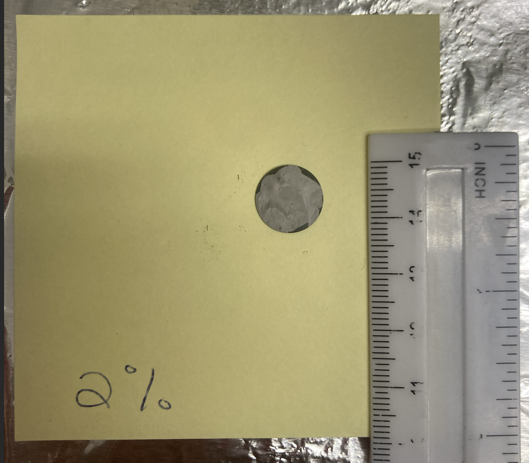
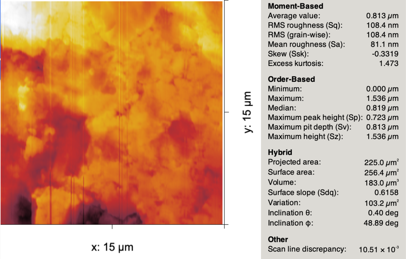
The cross-sectional surface area (needed to calculate conductivity) was found using ImageJ and given in the below table. The diameter of all pellets was approximately 11.9mm, but the electrode contact area was slightly smaller to avoid creating a short circuit along the sides of the pellet. To obtain the adjusted sample-electrode contact surface area, the average of the top and bottom electrode surface area was multiplied by the specific surface area as obtained from several AFM micrographs of the heat-treated pellet samples. On average, the ratio of the planar surface area to the AFM-measured surface area was about $1.12$. An example of the values reported by Gwyddion for an AFM image is shown below.
| Composition | Electrode SAtop $(mm)^2$ | Electrode SAbottom $(mm)^2$ | SAadjusted $(mm)^2$ | Pellet Thickness $(mm)$ |
|---|---|---|---|---|
| 2% Cu-CeO2 | $100$ | $106$ | $115$ | $0.30$ |
| 4% Cu-CeO2 | $95$ | $102$ | $110$ | $0.30$ |
| 8% Cu-CeO2 | $98$ | $103$ | $113$ | $0.30$ |
from IPython.display import Image
Image("/Users/saam/Documents/n-Cu-CeO2 Research/Images and Figures for Poster/AFMmicrograph.png", width = 600)
To obtain the lattice conductivity values is now straightforward.
\(\sigma = \frac{L}{R_gA} \tag{8}\)
- $L$: sample thickness
- $R_g$: grain resistance (lattice resistance)
- $A$: SAadjusted
We can then plot these values using the Arrhenius equation,
\(\sigma T = \sigma_{0}e^{\frac{-E_a}{kT}} \tag{9}\)
- $\sigma_{0}$: pre-exponential factor
- $E_a$: activation energy of electronic conduction (maybe polaron hopping)
- $T$: temperature (homologous)
- $k$: Boltzmann constant
although values are often plotted in the alternative form
\[\ln(\sigma T) = \ln(\sigma_{0}) + \frac{-E_a}{kT} \tag{10}\]The following equations are taken from Arthur Nowick and Harry Tuller’s 1977 paper on the theory of small polaron hopping as a method of electronic conduction in reduced CeO2. The authors used both AC (impedance) and DC testing methods to obtain the conductivity, and considered the Seebeck coefficient as a means to determine whether there existed a relationship between the density of charge carriers, $n$, and the testing temperature. In support of the small polaron conduction model, they found no such relationship.
In the paper, the testing temperatures considered ranged from 200°C to 1100°C, and method of reduction was exposure to a reducing gas stream at elevated temperature. In this project, we only consider temperatures below 250°C, and the method of the reduction of cerium is aliovalent doping by copper. Because we anticipate the same method of conduction, I will use their equations for mobility and the polaron jump rate as they may be useful in comparison between our values and those found in other literature.
The mobility of a small polaron is empirically given by the following probabilistic jump-rate model (specific to a cubic lattice):
\[\mu = (1-c)ea^2\frac{\Gamma}{kT} \tag{11}\]- $c$: fraction of available sites occupied by an electron
- $e$: electron charge
- $a$: lattice parameter
- $\Gamma$: polaron jump rate (to a neighboring site)
Gamma is defined as follows:
\[\Gamma = P\nu_0 e^{\frac{-E_a}{kT}} \tag{12}\]- $P$: probabilty that the electron will move with the polaron. $P \approx 1$ in the adiabatic case.
- $\nu_0$: appropriate optical phonon frequency
The frequency of short-wavelength optical phonons responsible for the formation of polarons, $\nu_0$ is given as 330 fs (3.03 GHz) by this paper using fast transient adsorbance spectroscopy (FTAS).
Now we have a system of two equations:
\[\mu = \frac{\sigma}{ne} \tag{13}\]and
\[\mu = (1-\frac{n}{N})ea^2\frac{\Gamma}{kT} \tag{14}\]where $N$ is the fraction of available sites per unit volume. Since in small polarons in ceria, the electrons are localized on the cations, and the unit cell is FCC, we cna solve for $N$ thusly: $N = \frac{4}{(5.44 Å)^3} = 2.48•10^{28}$ per cubic meter.
Substituting yields
\[\frac{\sigma}{ne} = (1-\frac{n}{N})ea^2\frac{\Gamma}{kT} \tag{15}\]which we can now use to solve for n.
The Arrhenius Plot
from matplotlib.ticker import ScalarFormatter

#list form lattice resistance values
res_2p = np.array([3.0712e6, 1.9824e6, 1.7551e6])
res_4p = np.array([7.7422e6, 1.017e6, 0.38986e6])
res_8p = np.array([24.86e6, 0.490280e6, 0.207500e6])

#L=0.3mm, A depends on pellet, convert to cm
con_2p = 0.3*10/res_2p*115
con_4p = 0.3*10/res_4p*110
con_8p = 0.3*10/res_8p*113

print(con_2p*100)

#log (sigma*T)
Tscale = np.array([[373, 0, 0],[0, 423, 0],[0, 0, 473]])

#oT and log(oT), not used in graphing
oT_2p = np.multiply(Tscale, con_2p)
oT_2p = np.array([(oT_2p[0])[0], (oT_2p[1])[1], (oT_2p[2])[2]])
log_oT_2p = np.log10(oT_2p)

oT_4p = np.multiply(Tscale, con_4p)
oT_4p = np.array([(oT_4p[0])[0], (oT_4p[1])[1], (oT_4p[2])[2]])
log_oT_4p = np.log10(oT_4p)

oT_8p = np.multiply(Tscale, con_8p)
oT_8p = np.array([(oT_8p[0])[0], (oT_8p[1])[1], (oT_8p[2])[2]])
log_oT_8p = np.log10(oT_8p)


Tinv = np.array([0.002680965147, 0.002364066194, 0.002114164905])


# introduce the axis first
fig, arrplot = plt.subplots(dpi=120)
arrplot.plot(Tinv*1000, con_2p, label = '[Cu] = 0.02', color = '#e0f279', marker = 'o', linestyle = 'dashed')
arrplot.plot(Tinv*1000, con_4p, label = '[Cu] = 0.04', color = '#b5c45e', marker = 'o', linestyle = 'dashed')
arrplot.plot(Tinv*1000, con_8p, label = '[Cu] = 0.08', color = '#8d9949', marker = 'o', linestyle = 'dashed')

#find the activation energy (eV)
a, b = np.polyfit(Tinv, log_oT_8p, 1)
Ea = a * -8.617333e-5
#print(a)
#print(b)
print('pre-exp: ', np.exp(b))
print('Ea: ', Ea)

plt.xlabel('$1000/T$ (K$^{-1}$)')
plt.ylabel('$\sigma$ (Ω•cm)$^{-1}$')

plt.yscale("log")
plt.legend();
[0.01123339 0.01740315 0.019657  ]
pre-exp:  4375.731182577005
Ea:  0.3381231384376265
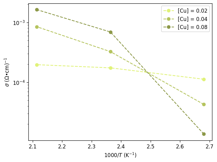
Table 1. Pre-exponential factor, activation energy, and the mobility, jump rate, and charge carrier density at 200 Celsius for different doping concentrations
| Cu (at. %) | $\sigma_0$ $(K/(\Omega•m))$ | $E_a$ $(eV)$ | $\mu$ $(200°C)$ $(cm^2/V•s)$ | $\Gamma$ $(200°C)$ $(s^{-1})$ | $n$ $(200°C)$ $(m^{-3})$ |
|---|---|---|---|---|---|
| 2% | $1.34$ | $0.05$ | $6.4•10^{-2}$ | $8.87•10^{11}$ | $1.90•10^{22}$ |
| 4% | $138$ | $0.21$ | $1.3•10^{-3}$ | $1.75•10^{10}$ | $4.16•10^{24}$ |
| 8% | $4376$ | $0.34$ | $5.2•10^{-5}$ | $7.22•10^{8}$ | $1.96•10^{26}$ |
For reference, the number of unit cells per cubic meter of single crystal cerium oxide is $6.21•10^{27}$